Metals can trap and concentrate light into volumes far smaller than the wavelength of light itself, a phenomenon known as plasmon resonance. This remarkable ability underpins a wide range of technologies, from ultrasensitive chemical sensors and cancer diagnostics to sub-wavelength photonic circuits and metasurface-based optical components. At the heart of this behaviour lies the plasma frequency of the metal, which is set by its free-electron concentration and has conventionally been considered fixed once the material composition is chosen. While researchers have used nanostructuring and dielectric engineering to indirectly adjust plasmonic properties, directly modifying the plasma frequency through mechanical deformation had remained largely unexplored.
Scientists at Jawaharlal Nehru Centre for Advanced Scientific Research (JNCASR), an autonomous institute of the Department of Science and Technology (DST), used epitaxial ultrathin titanium nitride (TiN) films to isolate the role of strain on plasmonic behaviour. TiN is a refractory material with a gold-like plasmonic response, superior thermal and chemical stability, and full compatibility with complementary metal-oxide-semiconductor (CMOS) chip fabrication. Two otherwise identical 10-nanometre-thick TiN films were grown, one strain-free on a magnesium oxide (MgO) substrate, and one subject to a controlled in-plane tensile strain induced by an aluminium scandium nitride (Al0.3Sc0.7N) buffer layer with a larger crystal lattice constant.
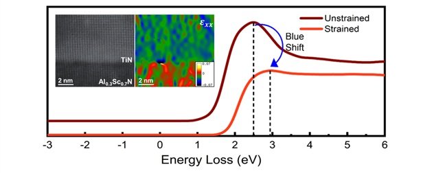
Using electron energy loss spectroscopy (EELS) in a scanning transmission electron microscope, Diksha Dadhich and co-workers in Prof. Bivas Saha’s group mapped the plasmon resonance energy at near-atomic spatial resolution across both films. The strained TiN film exhibited a pronounced blue shift of 0.30–0.45 electron volts in its plasmon resonance relative to the unstrained film, a large and spatially resolved shift that tracked the local strain distribution within the material. Both screened and unscreened plasmon modes shifted consistently, providing strong evidence that strain was directly modifying the intrinsic electronic response of the metal.
To understand the origin of this effect, the team performed first-principles density functional theory (DFT) calculations which revealed that tensile strain systematically lowers the energy required to form nitrogen vacancies in TiN. These vacancies act as electron donors, increasing the free-electron concentration and thereby raising the plasma frequency, explaining the experimentally observed blue shift. Spectroscopic ellipsometry and high-resolution X-ray diffraction measurements provided additional corroboration of this mechanism.
“Our work shows that strain is a powerful and previously underexplored control knob for plasmonic properties in metals. The ability to mechanically reconfigure the optical response of a CMOS-compatible material like TiN transforms plasmonics from a static platform to an active and programmable one, with exciting implications for on-chip photonics and optical sensing,” said Prof. Bivas Saha, corresponding author and Associate Professor at JNCASR.
Apart from JNCASR, Dr. Magnus Garbrecht, Vijay Bhatia, and Ashalatha Indiradevi Kamalasanan Pillai from the University of Sydney, Australia, participated in this research.
Discover more from News Link360
Subscribe to get the latest posts sent to your email.